High quality factory Precision Casting Wax for Mexico Importers

High quality factory
 Precision Casting Wax for Mexico Importers

Short Description:

Product Detail

Product Tags

Our mission is to become an innovative supplier of high-tech digital and communication devices by providing value added design, world-class manufacturing, and service capabilities for Radiator Valve Kit , Gas Smoker Automatic Temperature Control , Thermal Actuator , Warmly welcome to cooperate and develop with us! we are going to continue to provide product or service with high quality and competitive rate.
High quality factory Precision Casting Wax for Mexico Importers Detail:

Precision Casting Wax mainly is used for precision mechanical process with zero allowance or very limited allowance. We can not adopt general casting technique, but can only adopt zero allowance casting or precision casting. Because of the product’s structure is very delicate and complex especially in bejeweled with golden and silver, such as diamond ring, brooch, earring etc.

The characteristics of precision casting wax are: good coating property, no denaturalization to be heated, good flow ability, good thermal stability, and well surface finish.

0170411100427


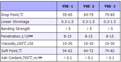
Product detail pictures:

High quality factory
 Precision Casting Wax for Mexico Importers detail pictures


We're going to commit ourselves to giving our esteemed buyers using the most enthusiastically considerate solutions for High quality factory Precision Casting Wax for Mexico Importers, The product will supply to all over the world, such as: Malaysia , Madagascar , Florida , Welcome to visit our company, factory and our showroom where displays various hair products that will meet your expectation. Meanwhile, it is convenient to visit our website, and our sales staff will try their best to provide you the best service. Please contact us if you need more information. Our aim is to help customers realize their goals. We are making great efforts to achieve this win-win situation.


  • This lecture introduces to the domain of Smart materials, their classification, advantages, direct and reverse effects.


    Silicon lens for mounting plasmonic photoconductive terahertz emitters sales@dmphotonics.com

    Featured research:

    Design, Fabrication, and Experimental Characterization of Plasmonic Photoconductive Terahertz Emitters

    In this video article we present a detailed demonstration of a highly efficient method for generating terahertz waves. Our technique is based on photoconduction, which has been one of the most commonly used techniques for terahertz generation 1-8. Terahertz generation in a photoconductive emitter is achieved by pumping an ultrafast photoconductor with a pulsed or heterodyned laser illumination. The induced photocurrent, which follows the envelope of the pump laser, is routed to a terahertz radiating antenna connected to the photoconductor contact electrodes to generate terahertz radiation. Although the quantum efficiency of a photoconductive emitter can theoretically reach 100%, the relatively long transport path lengths of photo-generated carriers to the contact electrodes of conventional photoconductors have severely limited their quantum efficiency. Additionally, the carrier screening effect and thermal breakdown strictly limit the maximum output power of conventional photoconductive terahertz sources. To address the quantum efficiency limitations of conventional photoconductive terahertz emitters, we have developed a new photoconductive emitter concept which incorporates a plasmonic contact electrode configuration to offer high quantum-efficiency and ultrafast operation simultaneously. By using nano-scale plasmonic contact electrodes, we significantly reduce the average photo-generated carrier transport path to photoconductor contact electrodes compared to conventional photoconductors 9. Our method also allows increasing photoconductor active area without a considerable increase in the capacitive loading to the antenna, boosting the maximum terahertz radiation power by preventing the carrier screening effect and thermal breakdown at high optical pump powers. By incorporating plasmonic contact electrodes, we demonstrate enhancing the optical-to-terahertz power conversion efficiency of a conventional photoconductive terahertz emitter by a factor of 50 10.

    Introduction
    We present a novel photoconductive terahertz emitter that uses a plasmonic contact electrode configuration to enhance the optical-to-terahertz conversion efficiency by two orders of magnitude. Our technique addresses the most important limitations of conventional photoconductive terahertz emitters, namely low output power and poor power efficiency, which originate from the inherent tradeoff between high quantum efficiency and ultrafast operation of conventional photoconductors.

    One of the key novelties in our design that led to this leapfrog performance improvement is to design a contact electrode configuration that accumulates a large number of photo-generated carriers in close proximity to the contact electrodes, such that they can be collected within a sub-picosecond timescale. In other words, the tradeoff between photoconductor ultrafast operation and high quantum efficiency is mitigated by spatial manipulation of the photo-generated carriers. Plasmonic contact electrodes offer this unique capability by (1) allowing light confinement into nanoscale device active areas between the plasmonic electrodes (beyond diffraction limit), (2) extraordinary light enhancement at the metal contact and photo-absorbing semiconductor interface 10, 11. Another important attribute of our solution is that it accommodates large photoconductor active areas without a considerable increase in the parasitic loading to the terahertz radiating antenna. Utilizing large photoconductor active areas enable mitigating the carrier screening effect and thermal breakdown, which are the ultimate limitations for the maximum radiation power from conventional photoconductive emitters. This video article is concentrated on the unique attributes of our presented solution by describing the governing physics, numerical modeling, and experimental verification. We experimentally demonstrate 50 times higher terahertz powers from a plasmonic photoconductive emitter in comparison with a similar photoconductive emitter with non-plasmonic contact electrodes.

    Keywords: Physics, Issue 77, Electrical Engineering, Computer Science, Materials Science, Electronics and Electrical Engineering, Instrumentation and Photography, Lasers and Masers, Optics, Solid-State Physics, Terahertz, Plasmonic, Time-Domain Spectroscopy, Photoconductive Emitter, electronics

    https://www.ncbi.nlm.nih.gov/pmc/articles/PMC3731459/

    Send your message to us:

    INQUIRY NOW
    • * CAPTCHA: Please select the Heart

    Related Products

    INQUIRY NOW
    • * CAPTCHA: Please select the Tree

    WhatsApp Online Chat !